
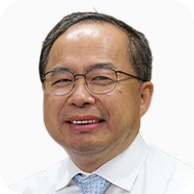
KAIST, Korea
Dr. Joungho Kim received B.S. and M.S. degrees in electrical
engineering from Seoul National University, Seoul, Korea, in
1984 and 1986, respectively, and Ph.D degree in electrical
engineering from the University of Michigan, Ann Arbor, in
1993. In 1994, he joined Memory Division of Samsung
Electronics, where he was engaged in Gbit-scale DRAM design.
In 1996, he moved to KAIST (Korea Advanced Institute of
Science and Technology). He is currently professor at
electrical engineering department of KAIST and the joint
faculty member of KAIST AI college. And he is the Director of
Graduate School of Computer Architect at KAIST. He serves as
the director of Samsung Industry Collaboration Center.
Recently, his research is focusing on the development of HBM
and HBF Architectures for next generation AI computing. In
addition, he is working on Deep Reinforcement Learning Methods
for the optimal design of high-speed channels and the delivery
networks in HBM, HBF, and AI computer modules. Furthermore,
his research centers on signal integrity and power integrity
modeling, design, and measurement methodologies for HBM, HBF,
3D IC, TSV, Interposer, and System-in-Packages. He has
authored and co-authored over 659 technical papers published
at refereed journals and conference proceedings. Also, he has
given more than 267 invited talks and tutorials at the
academia and the related industries. He is currently the
director of Samsung-KAIST industrial Collaboration Center.
He published a book, “Electrical Design of Through
Silicon Via,” by Springer in 2014. Dr. Joungho Kim was
Conference chair of IEEE EDAPS 2015 in Seoul, and Joint
conference chair of Japan-Korea Microwave society in 2015. He
also was the conference chair of IEEE WPTC (Wireless Power
Transfer Conference) 2014, held in Jeju Island, Korea. And he
was the symposium chair of IEEE EDAPS Symposium 2008, and was
the TPC chair of APEMC 2011. He is also an associated editor
of the IEEE Transactions of Electromagnetic Compatibility. He
served as a guest editor of the special issue in the IEEE
Transactions of Electromagnetic Compatibility for PCB level
signal integrity, power integrity, and EMI/EMC in 2010, and as
a guest editor of the special issue in the IEEE Transactions
of Advanced Packaging for TSV (Through-Silicon-Via) in 2011.
He served as a guest editor of the mini-special issue in the
IEEE Transactions of Microwave Theory and Techniques, for IEEE
WPTC in 2015. He received Outstanding Academic Achievement
Faculty Award of KAIST in 2006, KAIST Grand Research Award in
2008, National 100 Best Project Award in 2009, KAIST
International Collaboration Award in 2010, KAIST Grand
Research Award in 2014, and Teaching Award in 2015,
respectively. He was appointed as an IEEE EMC society
distinguished lecturer in a period from 2009-2011. He received
Technology Achievement Award from IEEE Electromagnetic Society
in 2010. He is currently IEEE fellow
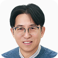
SK hynix, Korea
Dongkyun Kim is a Professor at SK hynix University. Until 2025, he served as Vice President and Fellow at SK hynix, where he led the Next-Generation Memory Architecture team for DRAM design. He received his B.S. and M.S. degrees in Information and Communication Engineering from Chungbuk National University, Korea, in 1993 and 1995, respectively. He joined Hynix in 1995 and has played a key role in the development of a broad range of DRAM technologies, including EDO, SDR, DDR1/2/3/4/5, LPDDR4/5, and HBM. Since 2012, he has been an active contributor to JEDEC task groups, participating in the definition and standardization of current and future DRAM specifications. Since January 2022, he has served as a Technical Program Committee (TPC) member of the ISSCC Memory Subcommittee. His current research and development interests center on next-generation memory and memory subsystems, with a particular emphasis on architectures and solutions for AI-driven computing.
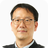
Samsung Electronics Co., Ltd.
Hoyoung Kim is a Master at Samsung Electronics — a prestigious designation reserved for the company's senior technical leaders — and serves as the Head of the CMP Group within the Foundry Process Development Team. He received his B.S. and M.S. degrees in Mechanical Engineering from Seoul National University before joining Samsung in 1999 as a CMP Engineer. With over 25 years of extensive expertise, he has spearheaded the development of CMP solutions across DRAM, Flash, and advanced Logic process integration, with a particular focus on next-generation foundry nodes including gate-all-around (GAA) technology. Throughout his career, he has built a prolific portfolio of more than 40 patents and publications spanning the full spectrum of CMP equipment, consumables, and processes, reflecting his long-standing commitment to advancing CMP technology in the semiconductor industry.
Organized by



Sponsored by